 English
 Español
 Deutsch
Industry News
Home / News / Industry News / Chinese Scientists Break Through Bottleneck! New Solar Cell Efficiency Soars to 10.44%
Copper Indium Sulfide (CuInS₂, CIS) is a chalcopyrite-structured semiconductor material in the I-III-VI₂ group. Recognized as a highly promising thin-film solar cell material in photovoltaics, it offers exceptional optoelectronic properties and environmental compatibility. Its key technical advantages include:

Image Source: Internet
Why Has This "Rising Star" of PV Materials Struggled to Commercialize?
Copper indium sulfide (CuInS₂) has been regarded as a rising star in the field of photovoltaics for many years. It can freely switch between n-type and p-type semiconductors by changing the sulfur content, and its bandgap perfectly matches the strongest visible spectrum range in sunlight.
Despite global efforts—including morphological engineering and heterojunction construction—CuInS₂solar cells remain confined to laboratories, with commercialization hindered by insufficient photoelectric conversion efficiency.
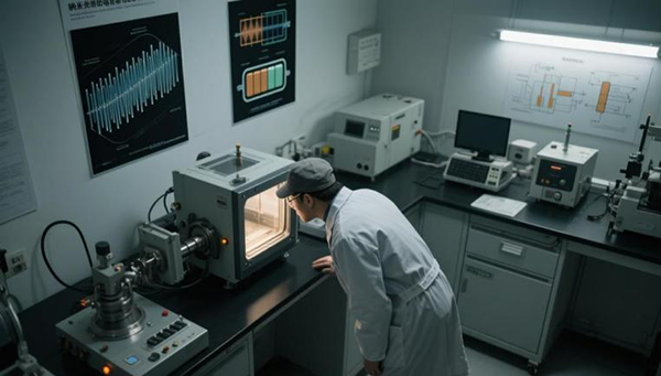
Image Source: Internet
CAS Team Solves "Nano-Ladder" Density Challenge
Researchers at the Hefei Institutes of Physical Science, Chinese Academy of Sciences (CAS), pioneered a solution using titanium dioxide nanorod arrays (TiO₂-NA). Traditional methods face a critical bottleneck: nanorod density, diameter, and length are interdependent, limiting device efficiency.
"Adjusting one parameter affects others—like deforming an entire ladder when modifying rung spacing," the team explained.
Breakthrough: Extended Hydrolysis Grows "Seeds"
By prolonging the hydrolysis of a precursor film, longer "gel chains" self-assemble into smaller anatase nanoparticles. These particles then convert in situ to rutile crystals during hydrothermal treatment, acting as "seeds" for nanorod growth. Precise control of hydrolysis enables independent tuning of nanorod density for the first time!
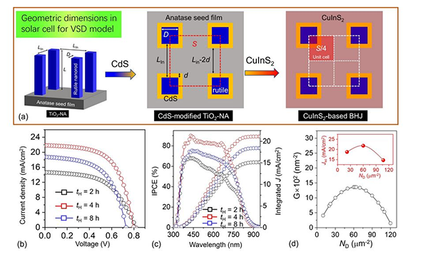
Image Source: Internet
Efficiency Reaches 10.44%! Model Reveals Success Mechanism
Integrating these density-tunable, dimensionally stable TiO₂-NA films into low-temperature-processed CuInS₂ solar cells achieved a record 10.44% power conversion efficiency under standard AM 1.5G illumination.
The team’s "Volume-Surface-Density" (VSD) model demonstrated how optimized nanorod spacing enhances light trapping, charge separation, and carrier collection.
"This research establishes a complete framework linking macro-process control, microstructural evolution, and device performance optimization," emphasized the scientists.
Dawn of Commercialization for Eco-Friendly PV Material
Published in the prestigious journal Small Methods, this study not only provides key technology to overcome CuInS₂ efficiency barriers but also pioneers a density-decoupling strategy that opens new design pathways for next-generation optoelectronic devices.
By constructing "density-tunable photoelectric ladders" in the nano-realm, Chinese scientists have brought this long-touted eco-friendly material a critical step closer to commercial reality.


+86 0576-80730906


Industrial Zone, QinggangTown, Yuhuan, Taizhou, Zhejiang, China
Copyright©Sunpro Power All Rights Reserved.
Solar PV Panel Module Factory
